- 您现在的位置:买卖IC网 > Sheet目录327 > HW-V5-ML561-UNI-G (Xilinx Inc)EVALUATION PLATFORM VIRTEX-5
R
Hardware Schematic Diagram
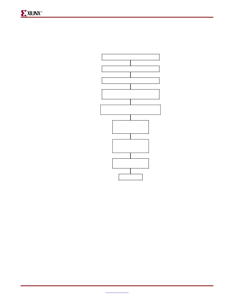
The voltage and contrast settings must be configured before the LCD panel is ready for
operation. Figure C-6 shows the initialization procedure required to set up the LCD
controller.
S et u p In s tr u ction Flow
Power ON
Bo a rd Power Su pply S t a rt
RE S ETB Pin i s Kept LOW
S t a rt FPGA Config u r a tion
RE S ETB Pin i s Kept LOW
FPGA Config u red a nd Applic a tion R u nning
RE S ETB Pin i s T a ken HIGH
ADC S elect
- ADC = 0 S EG1 --> S EG132
- ADC = 1 S EG132 --> S EG1
S HL S elect
- S HL = 0 COM1 --> COM64
- S HL = 1 COM64 --> COM1
ADC S elect
S HL S elect
LCD Bi as S elect
Volt a ge Converter ON
Volt a ge Reg u l a tor ON
Volt a ge Follower ON
Reg u l a tor Re s i s tor S elect
S et Reference Volt a ge
End Initi a liz a tion
LCD Bi as
DUTY0, 1 i s "11".
LCD Bi as 0 = 1/7
LCD Bi as 1 = 1/9
W a it longer th a n 1 m s b etween
e a ch in s tr u ction to let the volt a ge s s t ab ilize.
The on-chip re s i s tor s a re us ed.
Therefore, the s election MU S T b e
s et to 101.
S etting Reference Volt a ge
i s a two-p ass in s tr u ction:
- S et Reference Volt a ge Mode
- S et Reference Volt a ge Regi s ter
UG199_C_06_050106
Figure C-6:
LCD Controller Initialization Flow
Operation Example of the 6412 8 EFCBC- 3 LP
The KS0713 LCD controller has several default settings of operation on the LCD panel
PCB. Some settings are forced through direct bonding on the chip. The default settings are:
?
?
?
?
?
?
?
?
Master mode
Parallel mode
Internal oscillator
Duty cycle ratio is set to 1/65
Voltage converter input is between 2.4V ≤ VDD ≤ 3.6V, where VDD connects to 3.3V
Internal voltage divider resistors
Temperature coefficient is set to -0.05%/ ° C
Normal power mode is set
Virtex-5 FPGA ML561 User Guide
UG199 (v1.2.1) June 15, 2009
127
发布紧急采购,3分钟左右您将得到回复。
相关PDF资料
I-JET
JTAG ARM DEBUGGING PROBE
IAC24A
INPUT MODULE AC 5MA 24VDC
IAC5EQ
INPUT MODULE AC 10MA 5VDC
IB8RM
SURGE SUPP 8OUT 12'CORD W/REMOTE
IBAR12-20T
SURGE SUPPRSSR 20A 12OUT RACKMNT
IBAR12/20ULTRA
SURGE SUPPRSSR 20A 12OUT RACKMNT
IBAR12ULTRA
SURGE SUPPRSSR 15A 12OUT RACKMNT
IBAR12
SURGE SUPPRSSR 15A 12OUT RACKMNT
相关代理商/技术参数
HW-V5-ML561-UNI-G-J
功能描述:EVALUATION PLATFORM VIRTEX-5 RoHS:是 类别:编程器,开发系统 >> 通用嵌入式开发板和套件(MCU、DSP、FPGA、CPLD等) 系列:Virtex®-5 LXT 产品培训模块:Blackfin® Processor Core Architecture Overview
Blackfin® Device Drivers
Blackfin® Optimizations for Performance and Power Consumption
Blackfin® System Services 特色产品:Blackfin? BF50x Series Processors 标准包装:1 系列:Blackfin® 类型:DSP 适用于相关产品:ADSP-BF548 所含物品:板,软件,4x4 键盘,光学拨轮,QVGA 触摸屏 LCD 和 40G 硬盘 配用:ADZS-BFBLUET-EZEXT-ND - EZ-EXTENDER DAUGHTERBOARDADZS-BFLLCD-EZEXT-ND - BOARD EXT LANDSCAP LCD INTERFACE 相关产品:ADSP-BF542BBCZ-4A-ND - IC DSP 16BIT 400MHZ 400CSBGAADSP-BF544MBBCZ-5M-ND - IC DSP 16BIT 533MHZ MDDR 400CBGAADSP-BF542MBBCZ-5M-ND - IC DSP 16BIT 533MHZ MDDR 400CBGAADSP-BF542KBCZ-6A-ND - IC DSP 16BIT 600MHZ 400CSBGAADSP-BF547MBBCZ-5M-ND - IC DSP 16BIT 533MHZ MDDR 400CBGAADSP-BF548BBCZ-5A-ND - IC DSP 16BIT 533MHZ 400CSBGAADSP-BF547BBCZ-5A-ND - IC DSP 16BIT 533MHZ 400CSBGAADSP-BF544BBCZ-5A-ND - IC DSP 16BIT 533MHZ 400CSBGAADSP-BF542BBCZ-5A-ND - IC DSP 16BIT 533MHZ 400CSBGA
HW-V5-PCIE2-UNI-G
功能描述:KIT DEV PCIEXPRESS GTX VIRTEX5 RoHS:是 类别:编程器,开发系统 >> 通用嵌入式开发板和套件(MCU、DSP、FPGA、CPLD等) 系列:Virtex® -5 产品培训模块:Blackfin® Processor Core Architecture Overview
Blackfin® Device Drivers
Blackfin® Optimizations for Performance and Power Consumption
Blackfin® System Services 特色产品:Blackfin? BF50x Series Processors 标准包装:1 系列:Blackfin® 类型:DSP 适用于相关产品:ADSP-BF548 所含物品:板,软件,4x4 键盘,光学拨轮,QVGA 触摸屏 LCD 和 40G 硬盘 配用:ADZS-BFBLUET-EZEXT-ND - EZ-EXTENDER DAUGHTERBOARDADZS-BFLLCD-EZEXT-ND - BOARD EXT LANDSCAP LCD INTERFACE 相关产品:ADSP-BF542BBCZ-4A-ND - IC DSP 16BIT 400MHZ 400CSBGAADSP-BF544MBBCZ-5M-ND - IC DSP 16BIT 533MHZ MDDR 400CBGAADSP-BF542MBBCZ-5M-ND - IC DSP 16BIT 533MHZ MDDR 400CBGAADSP-BF542KBCZ-6A-ND - IC DSP 16BIT 600MHZ 400CSBGAADSP-BF547MBBCZ-5M-ND - IC DSP 16BIT 533MHZ MDDR 400CBGAADSP-BF548BBCZ-5A-ND - IC DSP 16BIT 533MHZ 400CSBGAADSP-BF547BBCZ-5A-ND - IC DSP 16BIT 533MHZ 400CSBGAADSP-BF544BBCZ-5A-ND - IC DSP 16BIT 533MHZ 400CSBGAADSP-BF542BBCZ-5A-ND - IC DSP 16BIT 533MHZ 400CSBGA
HW-VID-KIT
功能描述:可编程逻辑 IC 开发工具 Lattice Video Interface Kit
RoHS:否 制造商:Altera Corporation 产品:Development Kits 类型:FPGA 工具用于评估:5CEFA7F3 接口类型: 工作电源电压:
HW-VL1
制造商:IDEC CORPORATION 功能描述:BARRIER
HW-VL2
制造商:IDEC Corporation 功能描述:COVER;HW FNGR SAFE CONTAC CVR 制造商:IDEC CORPORATION 功能描述:HW FNGR SAFE CONTAC CVR
HW-VL3
制造商:IDEC Corporation 功能描述: 制造商:IDEC Corporation 功能描述:Replacs TW-VL3 FNGR SAF
HWW-X030T-10015Z-H1
制造商:P-TEC 制造商全称:P-tec Corporation 功能描述:X30T RGB LED Wall Washers
HWW-X030T-10015Z-H2
制造商:P-TEC 制造商全称:P-tec Corporation 功能描述:X30T RGB LED Wall Washers
